quienes somos

como el principal fabricante de material semiconductor compuesto en China. pam-xiamen desarrolla avanzadas tecnologías de epitaxia y crecimiento de cristales, desde la primera generación de obleas de germanio, arseniuro de galio de segunda generación con crecimiento de sustratos y epitaxia en materi7
Lee mas
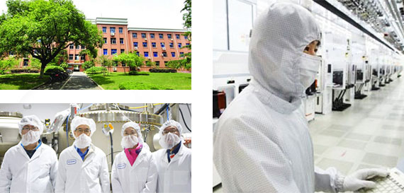
después de más de 20 años de acumulación y desarrollo, nuestra compañía tiene una ventaja obvia en innovación tecnológica y grupo de talentos. en el futuro, necesitamos acelerar el ritmo de acción real para proporcionar a los clientes mejores productos y servicios
doctor chan -Ceo de xiamen powerway material avanzado co., ltd

nuestros productos

láser azul

plantillas gan

Los productos de plantilla de pam-xiamen consisten en capas cristalinas de nitruro de galio (gan), nitruro de aluminio (aln), nitruro de aluminio y galio (algan) y nitruro de indio y galio (ingan), que se depositan en sustratos de zafiro. Los productos de plantilla de carburo de silicio o silicon.pam-xiamen permiten tiempos de ciclo de epitaxia 20-7

gan en silicio

sustrato de gan independiente

pam-xiamen ha establecido la tecnología de fabricación para la oblea de substrato gan independiente (de nitruro de galio), que es para uhb-led y ld. cultivado por tecnología de epitaxia en fase de vapor de hidruro (hvpe), nuestro sustrato gan tiene baja densidad de defectos.

gaas cristal

obleas de gaas (arseniuro de galio)

pwam desarrolla y fabrica sustratos semiconductores compuestos: cristal de arseniuro de galio y wafer.we ha utilizado tecnología avanzada de crecimiento de cristales, congelación de gradiente vertical (vgf) y tecnología de procesamiento de obleas gaas, estableció una línea de producción de crecimiento de cristales, corte, pulido para procesamiento 7

cristal sic

epitaxy sic

proporcionamos epitaxy sic personalizada de película delgada (carburo de silicio) sobre sustratos de 6h o 4h para el desarrollo de dispositivos de carburo de silicio. sic epi wafer se utiliza principalmente para diodos schottky, transistores de efecto de campo de semiconductores de óxido de metal, transistores de efecto de campo de unión, transisto7

cristal sic

sustrato sic

pam-xiamen ofrece obleas de carburo de silicio semiconductoras, 6h sic y 4h sic en diferentes grados de calidad para el investigador y fabricantes de la industria. hemos desarrollado la tecnología de crecimiento de cristal sic y la tecnología de procesamiento de obleas de cristal sic, estableció una línea de producción para el sustrato sic del fabr7

gan expitaxy

oblea epitaxial led basada gan

La oblea epitaxial con base en gan (nitruro de galio) de pam-xiamen es para el ultra alto brillo en diodos emisores de luz azul y verde (led) y diodos láser (ld).

gan hemt epitaxy

gan hemt oblea epitaxial

Los dobladillos de nitruro de galio (transistores de alta movilidad de electrones) son la próxima generación de tecnología de transistor de potencia rf. Gracias a la tecnología gan, pam-xiamen ahora ofrece algan / gan hemt epi wafer en zafiro o silicio, y algan / gan en plantilla de zafiro .

cristal sic

reclamo de oblea sic

pam-xiamen puede ofrecer los siguientes servicios de reclamo sic reclaim.

Por qué elegirnos

  • soporte de tecnología gratuito y profesional

    puede obtener nuestro servicio de tecnología gratuito desde la consulta hasta el servicio posterior basado en nuestro Más de 25 experiencias en la línea de semiconductores.

  • buen servicio de ventas

    nuestro objetivo es cumplir con todos sus requisitos, no importa cuán pequeñas sean las órdenes y cuán difíciles son las preguntas pueden ser, para mantener un crecimiento sostenido y rentable para cada cliente a través de nuestros productos calificados y un servicio satisfactorio.

  • Más de 25 años de experiencia

    con más que 25 + años experiencias en el campo de material semiconductor compuesto y en el negocio de exportación, nuestro equipo puede asegurarle que podemos entender sus requisitos y tratar su proyecto profesionalmente.

  • calidad confiable

    la calidad es nuestra primera prioridad. pam-xiamen ha sido iso9001: 2008 , posee y comparte cuatro modernas facories que pueden proporcionar una amplia gama de productos calificados para satisfacer las diferentes necesidades de nuestros clientes, y cada pedido tiene que ser manejado a través de nue7

"Hemos estado utilizando las obleas epidérmicas de powerway para algunos de nuestros trabajos. Estamos muy impresionados con la calidad de la epi".
james s.speck, departamento de materiales de la universidad de california
2018-01-25
"Queridos equipos de pam-xiamen, gracias por su opinión profesional, el problema fue resuelto, estamos muy contentos de ser su compañero"
raman k. chauhan, seren fotónica
2018-01-25
"gracias por la respuesta rápida de mis preguntas y el precio competitivo, es muy útil para nosotros, ordenaremos de nuevo pronto"
markus sieger, universidad de ulm
2018-01-25
"Las obleas de carburo de silicio han llegado hoy, ¡y estamos muy contentos con ellas! ¡Felicitaciones a su equipo de producción!"
dennis, universidad de exeter
2018-01-25

las universidades y empresas más famosas del mundo confían en nosotros

últimas noticias

Density Functional Theory Calculations of Atomic Configurations and Bandgaps of C-, Ge-, and Sn-Doped Si Crystals for Solar Cells

2020-03-17

Poly-Si crystals are mainly used in solar cells because of their low cost. Here, the zones of sensitivity to wavelengths in sunlight should be expanded to increase the engineering efficiency of solar cells. Group IV compound semiconductors films, e.g., Si (Ge) films doped with C, Ge (C, Si), and/or Sn atoms with contents of several %, on a Si or Ge substrate have been identified as potential solutions to this technical problem. In this study, we calculated the formation energy of each atomic configuration of C, Ge, and Sn atoms in Si by using density functional theory. The "Hakoniwa" method proposed by Kamiyama et al. [Materials Science in Semiconductor Processing, 43, 209 (2016)] was applied to a 64-atom supercell of Si including up to three atoms of C, Ge, and/or Sn (up to 4.56%) in order to obtain the ratio of each atomic configuration and the average value of the Si bandgaps. Not only the conventional generalized gradient approximation (GGA) but also the screened-exchange local-den...

Lee mas

Electrical Conductivity of Direct Wafer-Bonded GaAs/GaAs Structures for Wafer-Bonded Tandem Solar Cells

2020-03-09

Source:IOPscience For more information, please visit our website: www.semiconductorwafers.net, send us email at sales@powerwaywafer.com or powerwaymaterial@gmail.com

Lee mas

Optical Transmission, Photoluminescence, and Raman Scattering of Porous SiC Prepared from p-Type 6H SiC

2020-03-05

The optical transmission, temperature-dependence of the photoluminescence (PL), and Raman scattering of porous SiC prepared from p-type 6H-SiC are compared with those from bulk p-type 6H-SiC. While the transmission spectrum of bulk SiC at room temperature reveals a relatively sharp edge corresponding to its band gap at 3.03 eV, the transmission edge of porous SiC (PSC) is too wide to determine its band gap. It is believed that this wide edge might be due to surface states in PSC. At room temperature, the PL from PSC is 20 times stronger than that from bulk SiC. The PL PSC spectrum is essentially independent of temperature. The relative intensities of the Raman scattering peaks from PSC are largely independent of the polarization configuration, in contrast to those from bulk SiC, which suggests that the local order is fairly random. Source:IOPscience For more information, please visit our website: www.semiconductorwafers.net, send us email at sales@powerwaywafer.com&...

Lee mas

Upgrading of CdZnTe by annealing with pure Cd and Zn metals

2020-02-25

1−y alloy as the annealing source.

Lee mas

Fabrication of InP/SiO2/Si Substrate using Ion-Cutting Process and Selective Chemical Etching

2020-02-18

In this study, an InP layer was transferred onto a Si substrate coated with a thermal oxide, through a process combining ion-cutting process and selective chemical etching. Compared with conventional ion-cutting of bulk InP wafers, this layer transfer scheme not only takes advantage of ion- cutting by saving the remaining substrates for reuse, but also takes advantage of selective etching to improve the transferred surface conditions without using the chemical and mechanical polishing. An InP/InGaAs/InP heterostructure initially grown by MOCVD was implanted with H+ ions. The implanted heterostructure was bonded to a Si wafer coated with a thermal SiO2 layer. Upon subsequent annealing, the bonded structure exfoliated at the depth around the hydrogen projected range located in the InP substrate. Atomic force microscopy showed that after selective chemical etchings on the as-transferred structure, a final structure of InP/SiO2/Si was obtained with a relatively smooth surface. Source:IOPsc...

Lee mas

A review on MBE-grown HgCdSe infrared materials on GaSb (211)B substrates

2020-02-12

We review our recent efforts on developing HgCdSe infrared materials on GaSb substrates via molecular beam epitaxy (MBE) for fabricating next generation infrared detectors with features of lower production cost and larger focal plane array format size. In order to achieve high-quality HgCdSe epilayers, ZnTe buffer layers are grown before growing HgCdSe, and the study of misfit strain in ZnTe buffer layers shows that the thickness of ZnTe buffer layer needs to be below 300 nm in order to minimize the generation of misfit dislocations. The cut-off wavelength/alloy composition of HgCdSe materials can be varied in a wide range by varying the ratio of Se/Cd beam equivalent pressure during the HgCdSe growth. Growth temperature presents significant impact on the material quality of HgCdSe, and lower growth temperature leads to higher material quality for HgCdSe. Typically, long-wave infrared HgCdSe (x=0.18, cut-off wavelength of  at 80 K) presents an electron mobility as high as&nbs...

Lee mas

The Electrochemical Society Wet Etching Technology for Semiconductor and Solar Silicon Manufacturing: Part 2 - Process, Equipment and Implementation

2020-01-20

Wet etching is an important step in the manufacturing of semiconductor and solar wafers and for the production of MEMS devices. While it has been replaced by the more precise dry etching technology in advanced semiconductor device fabrication, it still plays an important role in the manufacture of the silicon substrate itself. It is also used for providing stress relief and surface texturing of solar wafers in high volume. The technology of wet etching silicon for semiconductor and solar applications will be reviewed. Impact on this step for wafer properties and critical parameters (flatness, topology and surface roughness for semiconductor wafers, surface texture and reflectance for solar wafers) will be presented. The rationale for the use of a etching technology and etchant for specific applications in semiconductor and solar wafer manufacturing will be presented. Source:IOPscience For more information, please visit our website: www.semiconductorwafers.net, send us email at&nbs...

Lee mas

Characterization of 4H-SiC Homoepitaxial Films on Porous 4H-SiC from Bis(trimethylsilyl)methane Precursor

2020-01-13

4H-SiC homoepitaxial films were grown on 8° off-axis porous 4H-SiC (0001) faces in the temperature range of  by chemical vapor deposition from bis(trimethylsilyl)methane (BTMSM) precursor. The activation energy for growth was 5.6 kcal/mol, indicating that the film growth is dominated by the diffusion-limited mechanism. Triangular stacking faults were incorporated in the SiC thin film grown at low temperature of 1280°C due to the formation of 3C-SiC polytype. Moreover, super-screw dislocations appeared seriously in the SiC film grown below 1320°C. Clean and featureless morphology was observed in the SiC film grown below 25 standard cubic centimeters per minute (sccm)  carrier gas flow rate of BTMSM at 1380°C while 3C-SiC polytype with double positioning boundaries grew at 30 sccm flow rate of BTMSM. The dislocation density of the epi layer was strongly influenced by the growth temperature and flow rate of BTMSM. Double axis crystal X-ray diffraction and optical micro...

Lee mas

Density Functional Theory Study of the Stress Impact on Formation Enthalpy of Intrinsic Point Defect around Dopant Atom in Ge Crystal

2020-01-07

During the last decade, the use of single crystal germanium (Ge) layers and structures in combination with silicon (Si) substrates has led to a revival of defect research on Ge. In Si crystals, dopants and stresses affect the intrinsic point defect (vacancy V and self-interstitial I) parameters and thus change the thermal equilibrium concentrations of V and I Source:IOPscience For more information, please visit our website: www.semiconductorwafers.net, send us email at sales@powerwaywafer.com or powerwaymaterial@gmail.com

Lee mas

Contáctenos

Si desea un presupuesto o más información sobre nuestros productos, por favor déjenos un mensaje, le responderemos lo antes posible.
   
Si desea un presupuesto o más información sobre nuestros productos, por favor déjenos un mensaje, le responderemos lo antes posible.